Home /
Expert Answers /
Electrical Engineering /
design-a-single-stage-common-emitter-bjt-amplifier-with-emitter-resistor-s-to-the-following-speci-pa819
(Solved): Design a single-stage Common-Emitter BJT amplifier with Emitter Resistor(s) to the following speci ...
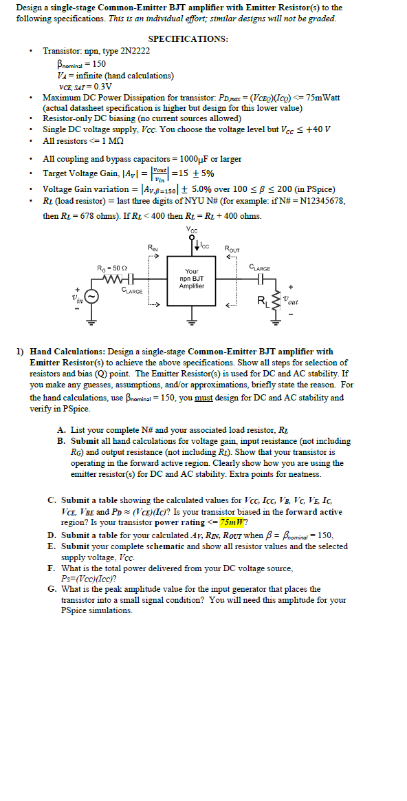
Design a single-stage Common-Emitter BJT amplifier with Emitter Resistor(s) to the following specifications. This is an individual effort; similar designs will not be graded. . SPECIFICATIONS: Transistor: npn, type 2N2222 Bnominal = 150 VA= infinite (hand calculations) VCE. SAR= 0.3V Maximum DC Power Dissipation for transistor: PD,max = (VCE)(I) <= 75mWatt (actual datasheet specification is higher but design for this lower value) Resistor-only DC biasing (no current sources allowed) Single DC voltage supply, Vcc. You choose the voltage level but vcc < +40 V All resistors C= 1 MO All coupling and bypass capacitors = 1000uF or larger Target Voltage Gain, |Ay1 = 1 =15 + 5% Vout Voltage Gain variation = |Av,B=150| + 5.0% over 100 SB < 200 (in PSpice) RL (load resistor) = last three digits of NYU N# (for example: if N#= N12345678, then RL = 678 ohms). If Rz < 400 then Rz = R1 + 400 ohms. = = Voc Ilcc RN -> ROUT CLARGE R = 50 WHH CLARGE Your non BJT Amplifier + RL out 1) Hand Calculations: Design a single-stage Cominon-Emitter BJT amplifier with Emitter Resistor(s) to achieve the above specifications. Show all steps for selection of resistors and bias (Q) point. The Emitter Resistor(s) is used for DC and AC stability. If you make any guesses, assumptions, and/or approximations, briefly state the reason. For the hand calculations, use Bnominal = 150, you must design for DC and AC stability and verify in PSpice. A. List your complete N# and your associated load resistor, RL B. Subunit all hand calculations for voltage gain, input resistance (not including RG) and output resistance (not including Rz). Show that your transistor is operating in the forward active region. Clearly show how you are using the emitter resistor(s) for DC and AC stability. Extra points for neatness. C. Subinit a table showing the calculated values for Vac, Icc, VB, VC, VE, IC, VCE, VBE and PD (CE) (Ic)? Is your transistor biased in the forward active region? Is your transistor power rating <= 75m? D. Submit a table for your calculated Av, Ran, Rout when B = Brominai = 150, E. Submit your complete schematic and show all resistor values and the selected supply voltage, Voc F. What is the total power delivered from your DC voltage source, Ps=(Vcc)(Icc)? G. What is the peak amplitude value for the input generator that places the transistor into a small signal condition? You will need this amplitude for your PSpice simulations.