Home /
Expert Answers /
Electrical Engineering /
instruction-answer-the-following-questions-using-the-ltspice-submit-the-ltspice-for-verification-pa894
(Solved): Instruction: Answer the following questions using the LTSPICE. Submit the LTSPICE for verification ...

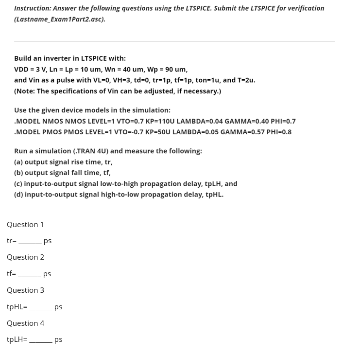
Instruction: Answer the following questions using the LTSPICE. Submit the LTSPICE for verification (Lastname_Exam1Part2.asc). Build an inverter in LTSPICE with: , and in as a pulse with , ton , and . (Note: The specifications of Vin can be adjusted, if necessary.) Use the given device models in the simulation: .MODEL NMOS NMOS LEVEL VTO LAMBDA .MODEL PMOS PMOS LEVEL VTO LAMBDA GAMMA Run a simulation (.TRAN ) and measure the following: (a) output signal rise time, tr, (b) output signal fall time, tf, (c) input-to-output signal low-to-high propagation delay, tpLH, and (d) input-to-output signal high-to-low propagation delay, tpHL.