Home /
Expert Answers /
Electrical Engineering /
please-answer-the-34-verify-your-design-34-part-thank-you-the-following-circuit-is-a-common-e-pa672
(Solved): Please answer the "verify your design" part. Thank you. The following circuit is a Common E ...
Please answer the "verify your design" part. Thank you. ????????
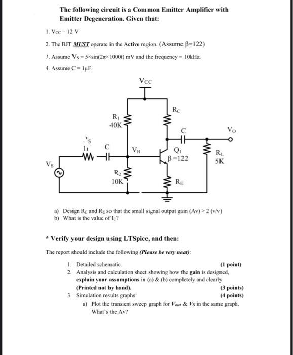

The following circuit is a Common Emitter Amplifier with Emitter Degeneration. Given that: 1. Vcc= 12 V 2. The BJT MUST operate in the Active region. (Assume B-122) 3. Assume Vs = 5xsin(2xx 1000t) mV and the frequency - 10kHz. 4. Assume C = 1µF. Vcc R? 40K www HHWW VB Rc WW C HH Q? B=122 R? SK R? 10K RE a) Design Re and Re so that the small signal output gain (Av) > 2 (v/v) b) What is the value of lc? * Verify your design using LTSpice, and then: The report should include the following (Please be very neat): 1. Detailed schematic. (1 point) 2. Analysis and calculation sheet showing how the gain is designed, explain your assumptions in (a) & (b) completely and clearly (Printed not by hand). (3 points) 3. Simulation results graphs: (4 points) a) Plot the transient sweep graph for Your & Vs in the same graph. What's the Av? WW Vo
b) Re-Plot (a) when Vin= 100×sin(2×1000t) mV, 1xsin(2xx1000t)V, and 2xsin(2x1000t)V separately. 4. Explain why as we increase the input voltage, the Vo signal is clipped. (1 point) 5. Conclusion and what you learned from this project. (1 point) • Note: The project is NOT for student pairs of two. Each student must do and submit the project individually.