(Solved): The circuit in Figure 1 is called a notch filter. Figure 2 shows the sketch of its Bode plot. Wh ...
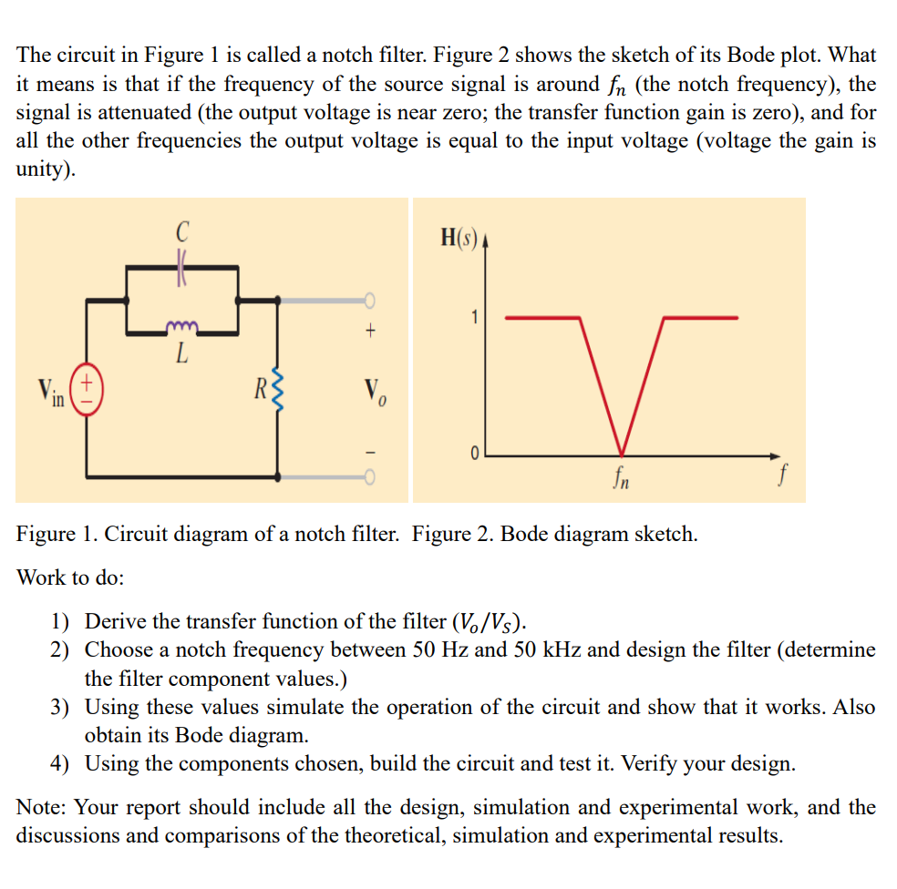
The circuit in Figure 1 is called a notch filter. Figure 2 shows the sketch of its Bode plot. What it means is that if the frequency of the source signal is around
f_(n)(the notch frequency), the signal is attenuated (the output voltage is near zero; the transfer function gain is zero), and for all the other frequencies the output voltage is equal to the input voltage (voltage the gain is unity). Figure 1. Circuit diagram of a notch filter. Figure 2. Bode diagram sketch. Work to do: Derive the transfer function of the filter
((V_(o))/(V_(S))). Choose a notch frequency between
50Hzand
50kHzand design the filter (determine the filter component values.) Using these values simulate the operation of the circuit and show that it works. Also obtain its Bode diagram. Using the components chosen, build the circuit and test it. Verify your design. Note: Your report should include all the design, simulation and experimental work, and the discussions and comparisons of the theoretical, simulation and experimental results. solve it for with detailed mathematical calculations and comaprision tables resistor 1kohm inductor 1mh capacitor 1nf