Home /
Expert Answers /
Electrical Engineering /
vhdl-figure-q3a-shows-the-circuit-diagram-of-a-full-adder-using-two-xor-gates-and-a-two-input-multi-pa554
(Solved): VHDL Figure Q3a shows the circuit diagram of a full adder using two XOR gates and a two input multi ...
VHDL
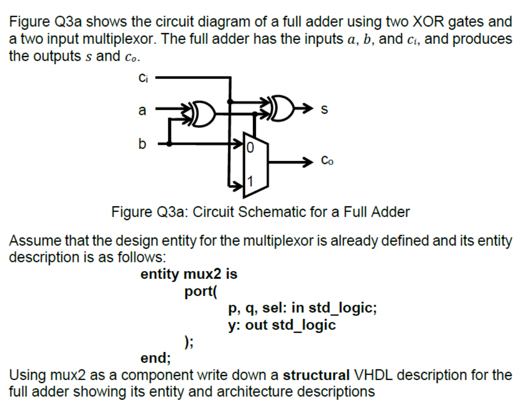
Figure Q3a shows the circuit diagram of a full adder using two XOR gates and a two input multiplexor. The full adder has the inputs \( a, b \), and \( c_{i} \), and produces the outputs \( s \) and \( c_{o} \). Figure Q3a: Circuit Schematic for a Full Adder Assume that the design entity for the multiplexor is already defined and its entity description is as follows: entity mux2 is port( p, q, sel: in std_logic; y: out std_logic end; Using mux2 as a component write down a structural VHDL description for the full adder showing its entity and architecture descriptions